The buck converter circuit and operation is already discussed here.

3. Buck Converter Analysis
The analysis of any converter involves in deriving the circuit output and input relation in terms of voltage and current equations, inductance and capacitance equations, and maximum stress across each component in circuit for its selection.
- Output and Input Voltage Relation
This relations can be derived from indcutor current and voltage principles
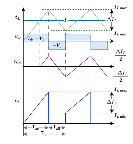
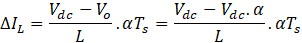
- The rate of change of current through inductor in both modes i.e. charge and discharge are equal and opposite i.e.


2. Inductor follows the volt-sec (voltage*time) balance principle i.e. average voltage across an inductor for one full cycle in steady state is zero.
Therefore,


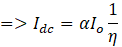
- Input and Output Current Relation
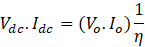
From the power balance equation of any ideal (lossless) electrical circuit is

But in practical circuits, lossless is not possible. Hence

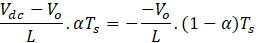
- Inductance Equation
The inductance value equation can be derive either from switch ON mode or switch OFF mode.
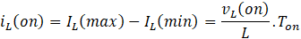
- From switch turn-on period, the ramp change in inductor current

2. From switch turn-off period, the ramp change in inductor current
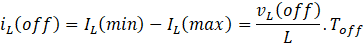
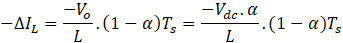
This is the minimum inductance value to be considered for desired output voltage and current.
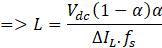
- Capacitance Equation
Current through capacitor in any mode of operation is


Q = charge = area of capacitor current in a half cycle
From capacitor current waveform (triangle shape),
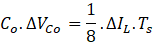

The minimum capacitor value that requires can be calculated using above equation.
- Minimum and Maximum Ratings of Component
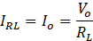
- Load
Average voltage across load,

Average current through load,
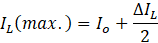
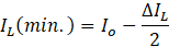
2. Inductor
Inductor current (AC+DC) always flowing through capacitor and load, here clear observation is load takes only DC component and capacitor allows only AC component. Therefore,
Average current through inductor,

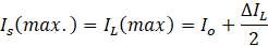
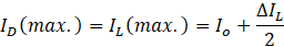
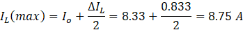
Maximum current through inductor,
Minimum current through inductor,
3. Capacitor
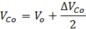
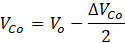
Average voltage across capacitor,

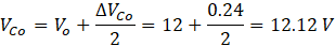
Maximum voltage across capacitor,
Minimum voltage across capacitor,
Maximum current through capacitor,

Minimum current through capacitor,

Average current through capacitor,

4. Switch
Average input/switch current,

Maximum input/switch current,
Maximum voltage across switch,

5. Diode
Average current through diode,

Maximum current through diode,
Maximum voltage across diode,

Based on maximum stress values from circuit analysis, each componenet should be selected for using in the circuit.
4. Buck Converter Design
The design example of buck converter is given below for clear understanding.
- Specifications
Input voltage, ![]()
Output voltage,
Output power,
Switching Frequency,
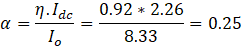
Efficiency,
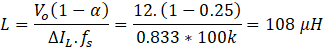
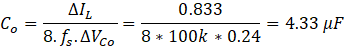
Voltage ripple,
Current ripple,
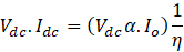
2. Input and Output Parameters
Input power,

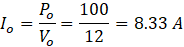
Input current,

Output current,
Duty cycle,

(or)
3. Current and voltage ripple
Average inductor current,

Inductor current ripple,

Average voltage across capacitor,

Capacitor voltage ripple,

4. Inductance and Capacitance
Minimum Inductance,
Minimum Capacitance,
5. Maximum Stress
Maximum voltage across switch

Maximum input/switch/diode/inductor current,
Average current through switch,

Maximum voltage across diode,

Average current through diode,

Maximum current through capacitor,

Maximum voltage across capacitor,
Leave a Reply