Circuit Diagram
The circuit diagram of single phase dual active bridge (DAB) resonant converter is shown in below Fig. This converter is useful in bidirectional power flow in battery charging and discharging applications.
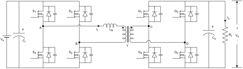
DAB consists of a full-bridge converters at input and output, resonant inductor, high-frequency transformer and load. High-frequency transformer provides galvanic isolation and can be useful to step-up and step-down available source to application requirement. Full-bridge converter at input side acts like an inverter and output side one acts a rectifier in battery charging mode. Similarly, a full-bridge converter at input side acts as rectifier and output side one acts as an inverter in battery discharging mode. MOSFET’s used as switches (![]() in primary side bridge, (
in primary side bridge, (![]() in secondary side bridge since the operating switching frequency in orders of kHz. The converter is designed to operate in lagging power factor mode to achieve zero-voltage switching (ZVS) for switches in primary and secondary side bridges. Power transfer happens in a dual-active bridge where two high-frequency square waves are created in the primary and secondary side of the transformer by the switching action of MOSFETs. These high-frequency square waves are phase shifted with respect to each other to take place the power flow action in the converter.
in secondary side bridge since the operating switching frequency in orders of kHz. The converter is designed to operate in lagging power factor mode to achieve zero-voltage switching (ZVS) for switches in primary and secondary side bridges. Power transfer happens in a dual-active bridge where two high-frequency square waves are created in the primary and secondary side of the transformer by the switching action of MOSFETs. These high-frequency square waves are phase shifted with respect to each other to take place the power flow action in the converter.
Advantages
- Bi-directional power flow capability
- Galvanic isolation
- Wide range voltage and load regulation
- Low load efficiency
Mostly Using Applications
- EV Chargers
- Renewable energy
- Battery energy storage
Leave a Reply