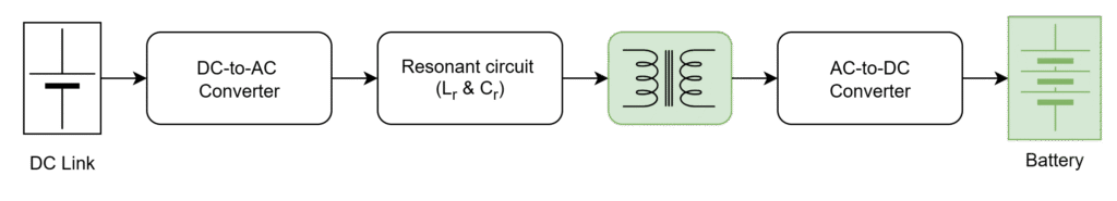
These are the mostly used PSFB topologies in different applications
- PSFB with Full-wave Rectifier
- PSFB with Full-bridge Rectifier
- PSFB with Synchronous Rectifier
- PSFB with Current Doubler
PSFB with Full-wave Rectifier
The circuit diagram is shown below
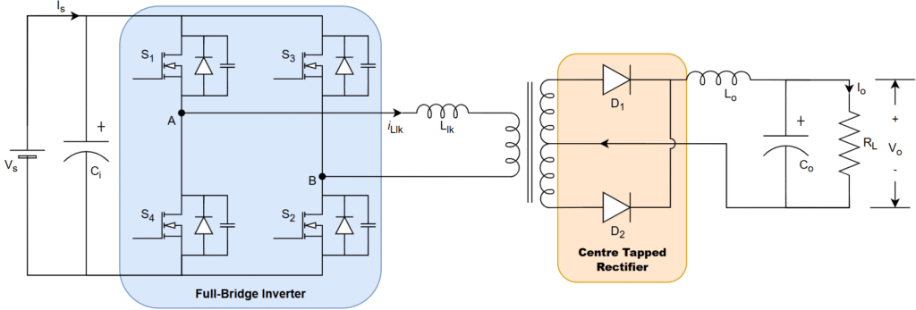
It is combination of full-bridge inverter (DC-AC), high-frequency transformer, and full-wave rectifier (AC-DC) with diodes.
PSFB with Full-bridge Rectifier
The circuit diagram is shown below
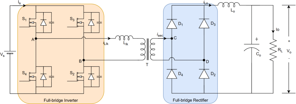
It is combination of full-bridge inverter (DC-AC), high-frequency transformer, and full-bridge rectifier (AC-DC) with diodes.
PSFB with Synchronous Rectifier (SR)
The circuit diagram is shown below
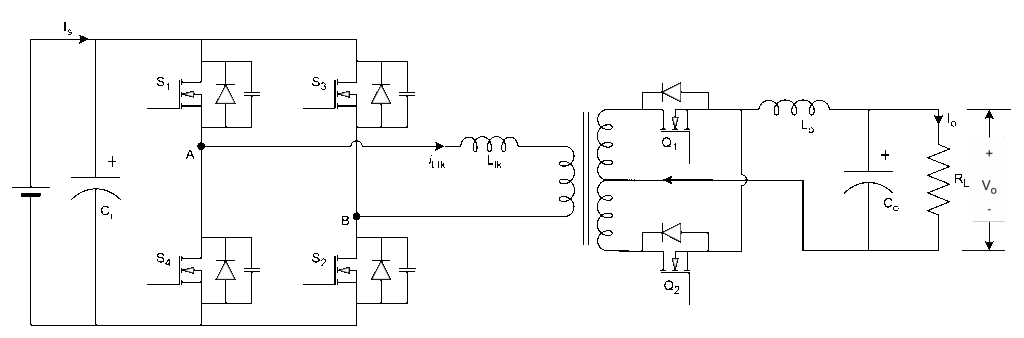
It is combination of full-bridge inverter (DC-AC), high-frequency transformer, and full-wave rectifier (AC-DC) with MOSFETS.
Here didoes are replaced by MOSFETS (Diode Vs SR MOSFET) for reducing the conduction losses and improves the efficiency particularly at high-current and low voltage output applications
PSFB with Current Doubler
The circuit diagram is shown below
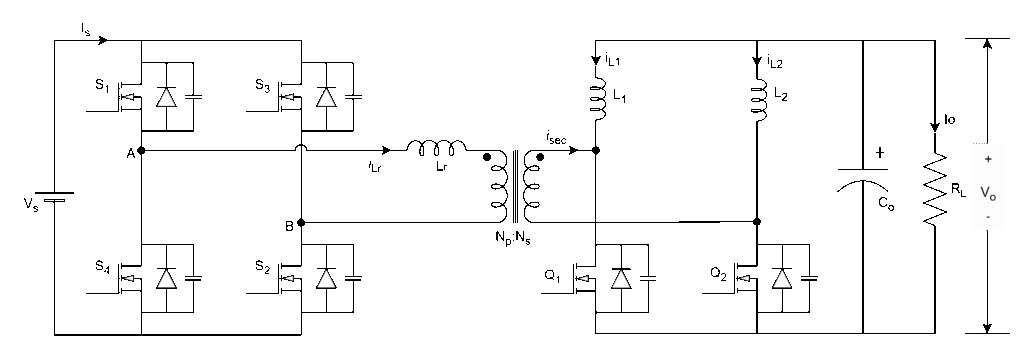
It is combination of full-bridge inverter (DC-AC), high-frequency transformer, and current doubler (AC-DC) with diodes/SR MOSFETs.
Current doubler circuit used to reduce the current ripple and improve the efficiency at high current applications
The PSFB circuit with current doubler and SR MOSFETs instead of diodes improves the overall converter efficiency by reducing the current ripple and conduction losses.
Leave a Reply