- Circuit Description
- Circuit Operation
- Circuit Analysis
- Circuit Design
Totem-pole PFC Circuit Analysis
The analysis of totem-pole PFC circuit involves mainly derive and design of the following components.
- Input inductor
- Output capacitor
- MOSFETs selection
- Diodes selection
- Input Inductor
When positive input voltage and currents, D2 always conduct; Q1 and Q2 conduct alternatively
- Q2 – ON for Ton period,


- Q1 – ON for Toff period
When negative input voltage and currents, D1 always conduct; Q1 and Q2 conduct alternatively
- Q1 – ON for Ton period,


- Q2 – ON for Toff period


In a full cycle period, the area of inductor charge and discharges in ON and OFF periods respectively of any switch is equal. Hence,

From Ts = Ton + Toff


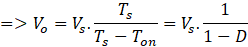
Duty cycle, D = Ton/Ts
From Q1 turn-on time period and above equation

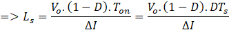
Where, current is the ripple of input AC peak current.
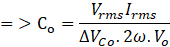
- Output Capacitor
DC Link capacitor is required to filter out the AC component at the output side. The instantaneous power drawn from grid is the in-phase voltage and currents with same frequency.


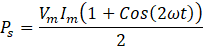

Therefore, the power has the both DC and AC components with a double the frequency. It creates the ripple in the output voltage at DC bus. The frequency of this ripple is double the switching frequency.
The ripple current through output capacitor,

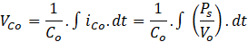
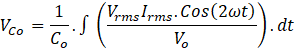
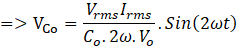
The ripple voltage across capacitor is the double the switching frequency with an amplitude of

Therefore, Output Capacitor
- MOSFETs Selection
The maximum voltage across MOSFET is DC bus voltage which appears across the output load and it may also includes ripple voltage. The maximum current flow through MOSFET is peak current of input inductor.
- Diode’s Selections
The maximum voltage across diode is DC bus voltage which appears across the output load and it may also includes ripple voltage. The maximum current flow through diode is peak current of input inductor.
Totem-pole PFC circuit Design
The design parameters for the totem-pole PFC circuit are given below.
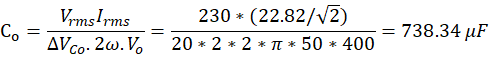
AC input voltage (RMS) : Vac : 80 – 230 – 264 V
Maximum AC line current (RMS) : Iac :16.2 A
Maximum Output power : Po : 3600 W (max.)
DC output voltage : Vdc : 400 V
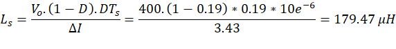
Switching frequency : fs : 66 kHz
Current ripple : Ir : 15% of peak input current
Voltage ripple : Vr : 5% of output voltage
Efficiency : 98%
Power factor: pf : > 0.99
The following steps should be followed to design an efficient converter and selection of device ratings.
Step-1: Calculation of maximum input current
- Maximum input power
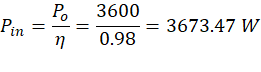
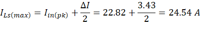
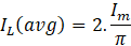
- Maximum peak input current
230 V considered since derating the power starts at this input voltage. Therefore, 230 V is the minimum input voltage where maximum input current occurs for rated power.
Step-2: Calculate the maximum allowable current and voltage ripples
- Current ripple

- Voltage ripple
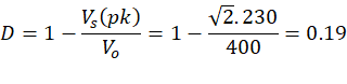
Step-3: Calculate the duty cycle
Step-4: Calculate the inductance value
Step-5: Calculate the capacitance value
Step-6: Devices maximum ratings for its selection
- Inductor
- High-frequency leg MOSFET
- The maximum voltage across MOSFET is DC bus voltage which is 400 V plus ripple voltage approximately 20 V i.e. 420 V.
- The maximum current flow through MOSFET is peak inductor current which is 24.54 A.
- Capacitor
- The maximum voltage across capacitor is DC bus voltage which is 400 V plus ripple voltage approximately 20 V i.e. 420 V.
- Diode
- The maximum voltage across capacitor is DC bus voltage which is 400 V plus ripple voltage approximately 20 V i.e. 420 V.
- The maximum current flow through diode is peak inductor current which is 24.54 A
Input inductance:
Output capacitance:
Leave a Reply